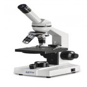
خرید سیستم مانیتورینگ میکروسکوب / فروش سیستم مانیتورینگ میکروسکوب
مشاهده سریع محصول
خرید سیستم مانیتورینگ میکروسکوب / فروش سیستم مانیتورینگ میکروسکوب
رزولوشن 12 مگاپیکسل
:حسگر BSI-CMOS با رزولوشن 12 مگاپیکسل
پردازشگر DIGIC 5
لرزشگیر هوشمند 5/4 مرحله ای
کنترل کامل عملیات
محدوده حساسیت از ISO 80 تا ISO 6400
قابلیت عکسبرداری با فرمت RAW
قابلیت تصویربرداری با کیفیت Full HD با صدای استریو و پورت HDMI
سرعت عکسبرداری پیوسته تا 13 فریم در ثانیه
مانیتور متحرک 2.8 اینچی
قابلیت نصب فلاش جداگانه و منظره یاب الکترونیک
خرید سیستم مانیتورینگ میکروسکوب / فروش سیستم مانیتورینگ میکروسکوب
سیستم مانیتورینگ میکروسکوپی / خرید مانیتورینگ میکروسکوپی / فروش مانیتورینگ میکروسکوپی / قیمت مانیتورینگ میکروسکوپی / CCD / خرید CCD / فرو شCCD / قیمت سیستم انتقال تصویر / خرید سیستم انتقال تصویر / فروش سیستم انتقال تصویر
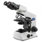
مدل :SX60
شرح کالا : دارای تصویر یک به یک با وضوح بالا و با انتقال تصویر ۶۰ فریم بر ثانیه
میزان بزرگنمایی لنز این دوربین ۵۰ برابر معادل فاصله کانونی ۱۲۰۰-۲۴ میلیمتر
رزولوشن ۱۲ مگاپیکسل
:حسگر BSI-CMOS با رزولوشن ۱۲ مگاپیکسل
پردازشگر DIGIC 5
لرزشگیر هوشمند ۵/۴ مرحله ای
کنترل کامل عملیات
محدوده حساسیت از ISO 80 تا ISO 6400
قابلیت عکسبرداری با فرمت RAW
قابلیت تصویربرداری با کیفیت Full HD با صدای استریو و پورت HDMI
سرعت عکسبرداری پیوسته تا ۱۳ فریم در ثانیه
مانیتور متحرک ۲٫۸ اینچی
قابلیت نصب فلاش جداگانه و منظره یاب الکترونیک
Introduction to Charge-Coupled Devices (CCDs)
Digital camera systems, incorporating a variety of charge-coupled device (CCD) detector configurations, are by far the most common image capture technology employed in modern optical microscopy. Until recently, specialized conventional film cameras were generally used to record images observed in the microscope. This traditional method, relying on the photon-sensitivity of silver-based photographic film, involves temporary storage of a latent image in the form of photochemical reaction sites in the exposed film, which only becomes visible in the film emulsion layers after chemical processing (development).
Figure 1 – Digital CCD Camera Systems for Optical Microscopy
Digital cameras replace the sensitized film with a CCD photon detector, a thin silicon wafer divided into a geometrically regular array of thousands or millions of light-sensitive regions that capture and store image information in the form of localized electrical charge that varies with incident light intensity. The variable electronic signal associated with each picture element (pixel) of the detector is read out very rapidly as an intensity value for the corresponding image location, and following digitization of the values, the image can be reconstructed and displayed on a computer monitor virtually instantaneously.
Several digital camera systems designed specifically for optical microscopy are illustrated in Figure 1. The Nikon Digital Eclipse DXM1200 provides high quality photo-realistic digital images at resolutions ranging up to 12 million pixels with low noise, superb color rendition, and high sensitivity. The camera is controlled by software that allows the microscopist a great deal of latitude in collecting, organizing, and correcting digital images. Live color monitoring on the supporting computer screen at 12 frames per second enables easy focusing of images, which can be saved with a choice of three formats: JPG, TIF, and BMP for greater versatility.
The DS-5M-L1 Digital Sight camera system (Figure 1) is Nikon’s innovative digital imaging system for microscopy that emphasizes the ease and efficiency of an all-in-one concept, incorporating a built-in LCD monitor in a stand-alone control unit. The system optimizes the capture of high-resolution images up to 5 megapixels through straightforward menus and pre-programmed imaging modes for different observation methods. The stand-alone design offers the advantage of independent operation including image storage to a CompactFlash Card housed in the control/monitor unit, but has the versatility of full network capabilities if desired. Connection is possible to PCs through a USB interface, and to local area networks or the Internet via Ethernet port. Web browser support is available for live image viewing and remote camera control, and the camera control unit supports HTTP, Telnet, FTP server/client, and is DHCP compatible. The camera systems illustrated in Figure 1 represent the advanced technology currently available for digital imaging with the optical microscope.
Perhaps the single most significant advantage of digital image capture in optical microscopy, as exemplified by CCD camera systems, is the possibility for the microscopist to immediately determine whether a desired image has been successfully recorded. This capability is especially valuable considering the experimental complexities of many imaging situations and the transient nature of processes that are commonly investigated. Although the charge-coupled device detector functions in an equivalent role to that of film, it has a number of superior attributes for imaging in many applications. Scientific-grade CCD cameras exhibit extraordinary dynamic range, spatial resolution, spectral bandwidth, and acquisition speed. Considering the high light sensitivity and light collection efficiency of some CCD systems, a film speed rating of approximately ISO 100,000 would be required to produce images of comparable signal-to-noise ratio (SNR). The spatial resolution of current CCDs is similar to that of film, while their resolution of light intensity is one or two orders of magnitude better than that achieved by film or video cameras. Traditional photographic films exhibit no sensitivity at wavelengths exceeding 650 nanometers in contrast to high-performance CCD sensors, which often have significant quantum efficiency into the near infrared spectral region. The linear response of CCD cameras over a wide range of light intensities contributes to the superior performance, and gives such systems quantitative capabilities as imaging spectrophotometers.
A CCD imager consists of a large number of light-sensing elements arranged in a two-dimensional array on a thin silicon substrate. The semiconductor properties of silicon allow the CCD chip to trap and hold photon-induced charge carriers under appropriate electrical bias conditions. Individual picture elements, or pixels, are defined in the silicon matrix by an orthogonal grid of narrow transparent current-carrying electrode strips, or gates, deposited on the chip. The fundamental light-sensing unit of the CCD is a metal oxide semiconductor (MOS) capacitor operated as a photodiode and storage device. A single MOS device of this type is illustrated in Figure 2, with reverse bias operation causing negatively charged electrons to migrate to an area underneath the positively charged gate electrode. Electrons liberated by photon interaction are stored in the depletion region up to the full well reservoir capacity. When multiple detector structures are assembled into a complete CCD, individual sensing elements in the array are segregated in one dimension by voltages applied to the surface electrodes and are electrically isolated from their neighbors in the other direction by insulating barriers, or channel stops, within the silicon substrate.
The light-sensing photodiode elements of the CCD respond to incident photons by absorbing much of their energy, resulting in liberation of electrons, and the formation of corresponding electron-deficient sites (holes) within the silicon crystal lattice. One electron-hole pair is generated from each absorbed photon, and the resulting charge that accumulates in each pixel is linearly proportional to the number of incident photons. External voltages applied to each pixel’s electrodes control the storage and movement of charges accumulated during a specified time interval. Initially, each pixel in the sensor array functions as a potential well to store the charge during collection, and although either negatively charged electrons or positively charged holes can be accumulated (depending on the CCD design), the charge entities generated by incident light are usually referred to as photoelectrons. This discussion considers electrons to be the charge carriers. These photoelectrons can be accumulated and stored for long periods of time before being read from the chip by the camera electronics as one stage of the imaging process.
Image generation with a CCD camera can be divided into four primary stages or functions: charge generation through photon interaction with the device’s photosensitive region, collection and storage of the liberated charge, charge transfer, and charge measurement. During the first stage, electrons and holes are generated in response to incident photons in the depletion region of the MOS capacitor structure, and liberated electrons migrate into a potential well formed beneath an adjacent positively-biased gate electrode. The system of aluminum or polysilicon surface gate electrodes overlie, but are separated from, charge carrying channels that are buried within a layer of insulating silicon dioxide placed between the gate structure and the silicon substrate. Utilization of polysilicon as an electrode material provides transparency to incident wavelengths longer than approximately 400 nanometers and increases the proportion of surface area of the device that is available for light collection. Electrons generated in the depletion region are initially collected into electrically positive potential wells associated with each pixel. During readout, the collected charge is subsequently shifted along the transfer channels under the influence of voltages applied to the gate structure. Figure 3 illustrates the electrode structure defining an individual CCD sense element.
دیدگاهها
هیچ دیدگاهی برای این محصول نوشته نشده است.